by John Reynolds
Introduction
 AMD’s initial foray into the realm of DX10 graphics landed with something of a thud — a late, underwhelming thud in the form of the R600 chip-based Radeon HD 2900 XT last summer. The R600 was a large, hot chip that failed to compete against NVIDIA’s GeForce 8800 GTX that had been released a full half-year earlier. AMD scrambled and responded with the RV670 chip, upon which the Radeon HD 3850 and HD 3870 boards were based. The RV670, while extremely derivative of the R600 in design, was moved to a 55nm manufacturing process and the subsequent die shrink saw a much smaller, cooler running GPU than the 2900 XT. The Radeon 3000 series was therefore more competitive in performance against NVIDIA products, and being based on a smaller chip was priced to move, putting AMD somewhat back into the GPU fray. NVIDIA, however, is not a company that sees kindly to its market share being threatened and responded with excellent products such as the GeForce 9600 GT, and with price drops for GPUs like the 8800 GT. As SimHQ’s recent Midrange GPU Roundup showed, this left AMD again taking backseat to NVIDIA’s products, and the graphics market has been waiting to see how the struggling company would respond.
The RV770 chip is AMD’s response and it’s a truly impressive engineering feat from a number of perspectives. The new chip has a die size increase of roughly 35% over that of the RV670 (256mm^2 vs. 190mm^2, and a transistor increase from 666m to 965m), yet AMD has managed to cram an amazing amount of increased functionality into the chip. While staying with a 55nm fabrication process, AMD has taken their previous architecture and increased the number of stream processors (shader units) from 320 to 800 units, more than doubled the texture units, completely revamped the memory controller, and beefed-up the ROPs (render back-end units). All of this suggests AMD’s engineers went back to the drawing board for major redesigns of the architecture to pack this much processing power into such a relatively small chip (NVIDIA’s G92, used for products like the 9800 GTX, is roughly 330mm^2 in size). How did AMD manage to pull this off? We’ll try to quickly cover the main improvements made to RV770 from the previous generation before diving into what most readers really want to see: the performance numbers.
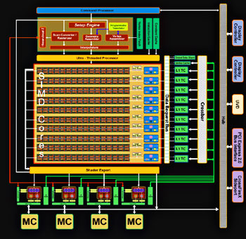 First off, AMD redesigned the stream processing units to be able to increase their head count from 320 to 800 units. These units are now arranged in 10 SIMD arrays, each sporting 80 cores and a 16KB cache. Each SIMD array also boasts four texture units with an L1 cache, and the shader units have of course been optimized for better performance, with each unit able to perform two operations per clock cycle (single-precision FP MAD and MUL ops). With this many stream processors clocked at the frequency of the Radeon HD 4850, 625MHz, AMD is able to claim the first desktop product that breaks the one teraflop barrier. All bundled in a $200 graphics board. Readers now can see why we described the RV770 as an impressive engineering feat a few sentences earlier. And considering how the potential use of graphics boards appears to be on the verge of ranging beyond just the rendering of 3D graphics, with the advent of physics, photo manipulation, video transcoding, folding@home projects, etc., becoming GPU-accelerated, the raw math-crunching power of the RV770 will certainly be put to good use by such applications. The Radeon HD 4870, clocked at a reported 750MHz, should offer a theoretical 1.2 teraflops at its $300 price point, and with its GDDR5 memory and the substantial memory bandwidth increase it brings should see its real-world usage come closer to theoretical peaks than the HD 4850.
Beyond the stream processors, AMD has also redesigned the memory controller. The old ring bus architecture introduced with the Radeon 1800/1900s and used up to the RV670 is now gone and has been replaced with a more distributed design that sees the interface placed around the chip’s edges and the controllers positioned closer to the ROPs. AMD claims that this improves bandwidth utilization while requiring less die space than the previous ring bus design. The new controllers also have an L2 cache with each block and support GDDR5. The Radeon HD 4850 uses GDDR3, but the new memory type will arrive with the HD 4870. Rumors have been circulating of a dual-chip R700 product coming in late summer or early fall and this new memory controller may suggest that AMD has worked to improve communication between chips compared to previous multi-GPU products.
Related Posts:
Related posts:
 ATI Radeon HD 4850 Performance Preview Page 2
ATI Radeon HD 4850 Performance Preview Page 3
ATI Radeon HD 4850 Performance Preview Page 4
ATI Radeon HD 4850 Performance Preview Page 5
ATI Radeon HD 4850 Performance Preview Page 6
ATI Radeon HD 4850 Performance Preview Page 2
ATI Radeon HD 4850 Performance Preview Page 3
ATI Radeon HD 4850 Performance Preview Page 4
ATI Radeon HD 4850 Performance Preview Page 5
ATI Radeon HD 4850 Performance Preview Page 6
 ATI Radeon HD 4870 Performance Preview
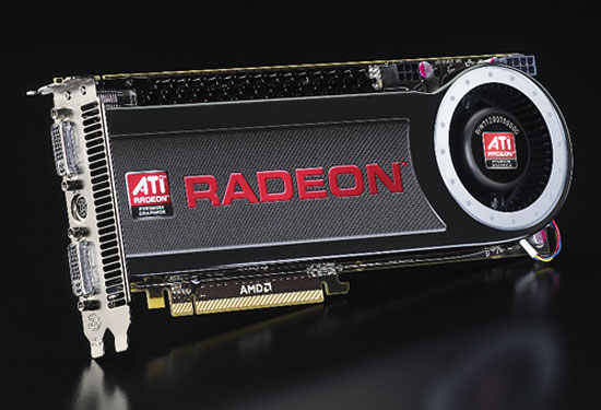 ATI Radeon HD 4870 X2 Performance Preview
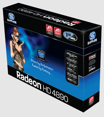 ATI Radeon® HD 4890 Performance Preview